Taking on Challenges in Integrated Photonics Packaging with Automated Assembly and Connection Technology
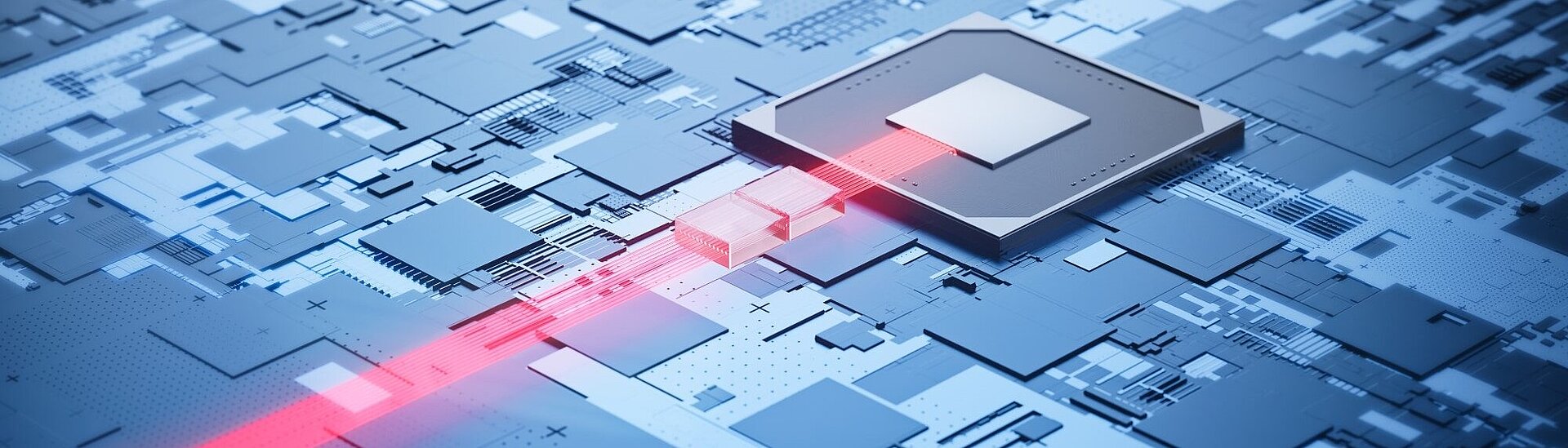
Testing, assembling, and packaging of photonic devices requires highly efficient systems. Alignment, especially array alignment, is one of the most significant cost factors, as it is essential at several stages of the production process to ensure throughput and manage production costs. For maximum performance, the optimal combination of accuracy, speed, and intelligent automation is needed. Positioning accuracies with submicron or nanometer precision, and in six degrees of freedom, are required.
Alignment speed and accuracy aside, other critical factors in testing, assembly, and packaging automation of photonic circuits include size constraints, heat dissipation, and reliability. The growing demand for smaller and more complex integrated photonics devices to meet the requirements of compact and portable electronic systems calls for assembly and packaging solutions that enable the integration of multiple optical components into densely packed modules while maintaining high performance and reliability. As photonics devices are often deployed in demanding environments, assembly and packaging systems must be able to ensure reliable performance while exposed to temperature extremes, mechanical shock, and vibration. With its diverse requirements, the silicon photonics market demands customization and flexibility in testing, assembly, and packaging solutions, making the availability of configurable and adaptable motion solutions necessary.
To improve the suitability of production processes for the complex automation tasks in silicon photonics applications, PI has developed a modular portfolio of solutions that are essentially based on two pillars: high-precision mechanical positioning systems, and algorithms to >> find first light and optimize coupling performance. Depending on the application requirements, different alignment solutions from PI can be used, detailed next.
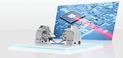
Multiple channels, multiple elements, and multiple interacting inputs and outputs, across multiple degrees of freedom, all requiring alignment optimization—a time-consuming and expensive task. PI’s Multi-Channel Photonics Alignment (FMPA) systems and unique proprietary alignment algorithms built into the controller automatically enable simultaneous alignments across multiple channels, devices, and degrees of freedom, optimizing overall array alignment in one quick step. Time and cost can be reduced by 99 % compared with traditional serial approaches.
When it comes to the alignment of fiber optic devices in high-volume production environments with strict cleanliness requirements, PI offers advanced motion solutions for fast, automated 24/7 operation based on different motor, guiding, and sensor technologies. Complemented by unique proprietary alignment algorithms for parallel optimization of any figure of merit, our solutions can increase throughput by more than one hundred times compared with traditional alignment systems.
Not all processes in photonic device production require maximum throughput and accuracy. Our portfolio also encompasses affordable alignment engines based on modular precision positioning stages that still benefit from PI’s high-performance motion controllers with award-winning embedded alignment algorithms.