Enabling High Functional Density of Printed Circuit Boards with Motion Control Solutions for Laser Drilling
Smartphone, smartwatch, tablet, industry electronics, electric car, camera and security systems, hearing aids, or pace makers – none of these technologies can do without the printed circuit board (PCB). It makes electronic devices come to life and makes trends in developments possible. The 6G cellular networks standard, autonomous driving, or M2M communication with their ever increasing data rates or quantities and high power densities cannot exist without the PCB. These trends set new standards for connectivity – it must be more functional, more compact, and more affordable.
Multilayer Assemblies and Finest Details Are Required
For this purpose, the design of PCBs, the materials, and the manufacturing processes must be optimized. Multilayer assemblies and increasingly finer details on increasingly smaller PCB surfaces are sought after in order to achieve a high level of integration. These multilayer designs have new requirements for the manufacturing process of the contacts, the so called vias, which connect the different layers.
This can only be realized by laser drilling. Particularly laser sources, whose wavelength can generate a small spot size and which is absorbed by the materials used in the circuit board, such as copper, polyimide, adhesives and resins, are suitable for a clean and fast generation of small deep holes. The UV laser, for example, emits a wavelength of 355 nm and offers small spot sizes of 15 to 25 μm, an excellent absorption, and high pulse rates.
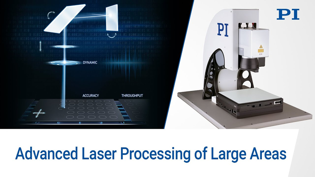
Galvonometer Scanner and Precision Mechanics Place Contacts Fast at the Right Position
In order to make use of the potential of UV laser sources, PI offers motion and laser control solutions that help laser machine builders, laser system integrators, and manufacturers to achieve the required throughput and the precision in production. For example, high-dynamics galvanometer scanners can be combined with high-precision linear motor stages in order to place the vias at the right position and to achieve the necessary vias per hour.
In close cooperation with leading manufacturers of galvanometer scanners, PI supports the development of core technologies in order to remove stitching errors, throughput restrictions, and precision deficiencies in the processing of large circuit boards. Combining these core technologies with our ACS motion controllers, positioning solutions, and application software make it possible for machine builders to build powerful systems that change the way the world connects and communicates.